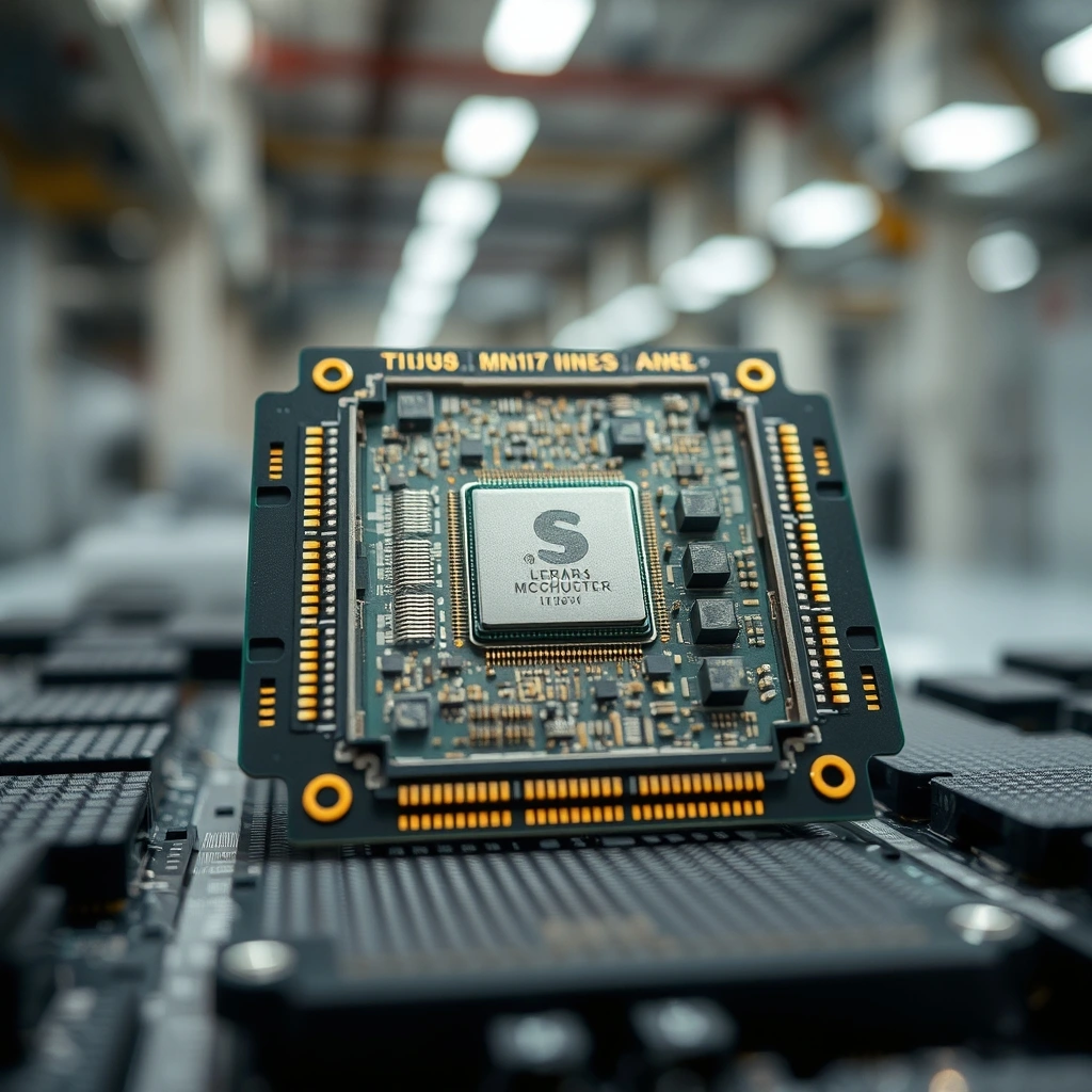
- The Memory Wall Rules All: Modern deep learning no longer chokes on mathematical compute; it chokes on memory bandwidth and electrical transfer costs.
- Custom Silicon is an Economic Shield: Hyperscalers are fleeing generic silicon margins by spinning proprietary inference accelerators to slash per-token running expenses.
- Packaging Beats Shrinking: With classical transistor scaling crawling to a halt, advanced 3D packaging and optical interconnects now drive generational performance jumps.
Walk into any modern enterprise datacenter, and the deafening shriek of cooling fans tells the whole story. Raw thermodynamic exhaustion has arrived. For three years, tech giants threw brute-force computing clusters at generative models, pretending power grids were infinite and liquid cooling loops were trivial. They are not. The industry is careening away from brute-force graphics processors toward hyper-specialized neural processing units, modular chiplets, and light-speed interconnects.
The Dirty Secret of AI Compute: The Memory Wall
Here is what hardware vendors whisper behind closed doors: raw math is basically free. Shuffling numbers across copper traces is where companies bleed cash. When a neural network processes billions of parameters, the actual floating-point matrix multiplications happen in picoseconds. Moving those weights from off-chip high-bandwidth memory to arithmetic logic units takes orders of magnitude more time and energy.
We call this the memory wall. It is ruthless. It dictates datacenter economics far more than raw clock speeds ever did. If your chip waits for weights to arrive, it burns idle power while producing zero tokens.
To survive this bottleneck, chip architects are ripping up conventional design blueprints. They are packing massive pools of static RAM directly adjacent to compute cores. They are stacking High Bandwidth Memory (HBM3e and early HBM4) vertically like skyscrapers, connected by microscopic silicon through-vias that reduce the physical distance electrons must crawl.
Beyond the Monolith: Why Chiplets Won the War
Single-die chips are hitting an impassable wall: the optical reticle limit. Lithography machines simply cannot print a single monolithic die much larger than roughly 858 square millimeters without catastrophic yield drops. Flaws creep in. Silicon wafers crack. Costs explode exponentially.
The solution? Break the processor into specialized fragments. Chiplets are now the undisputed standard for frontier hardware.
- Compute Tiles: Built on ultra-expensive 3nm or 2nm leading-edge nodes to handle brutal tensor math.
- I/O and Memory Controllers: Fabricated on mature, cost-effective 12nm nodes where bleeding-edge density adds zero value.
- Advanced Interposer Substrates: Bridging disparate silicon components using micro-bumps with microscopic spacing, tricking software into seeing a single cohesive processor.
By disaggregating components, manufacturers salvage yields and dial in custom silicon configurations without betting the entire company on a single giant die.
The In-House Silicon Rebellion Inside Big Tech
Let's be candid about the enterprise market: paying an eighty percent gross margin to a third-party merchant silicon vendor is unsustainable. Cloud hyperscalers realized this early. They are rapidly becoming semiconductor powerhouses in their own right, designing domain-specific accelerators engineered specifically for their proprietary software stacks.
Amazon has Trainium and Inferentia. Google relies heavily on its Tensor Processing Unit lines. Meta pushes forward with its MTIA architecture. Microsoft is deploying Maia. These designs strip away the legacy baggage of graphics processing pipelines—display engines, ray tracing units, rasterizers—leaving pure, unadulterated tensor processing engines.
| Design Dimension | General-Purpose GPUs | Next-Gen Custom NPUs | Photonic & Analog Cores |
|---|---|---|---|
| Primary Focus | Extreme flexibility & training versatility | Low-latency inference & per-token efficiency | Ultra-high-speed linear matrix math |
| Thermal Footprint | 400W – 1000W+ per package | 150W – 350W per socket | Under 75W (specialized) |
| Memory Strategy | Monolithic HBM complexes | Deep SRAM caches & pooled memory tiers | Direct optical feed buffers |
| Software Stack | Dominant proprietary ecosystems | Tailored compilers (Triton, OpenXLA) | Custom exploratory toolchains |
These custom inference chips excel at one specific job: churning through real-time user prompts at fraction-of-a-cent operational costs. When deploying hundreds of thousands of accelerators, cutting fifty watts per chip translates directly into tens of millions of dollars saved in annual utility bills.
Do not evaluate hardware solely on advertised Tera-Operations Per Second (TOPS). Without knowing the operational intensity and memory bus saturation rates, raw TOPS metrics are marketing theater. A chip with half the computational throughput but twice the memory bandwidth will run modern autoregressive models faster almost every single time.
Photons Over Electrons: The Optical Interconnect Shift
Copper wire has served humanity well, but it is choking on modern bandwidth demands. At ultra-high frequencies, copper generates brutal heat, suffers signal degradation over mere inches, and introduces latency spikes that throttle distributed clusters containing tens of thousands of compute nodes.
Enter silicon photonics and co-packaged optics (CPO). Instead of driving high-voltage electrical signals across traditional circuit boards to separate optical transceivers, engineers are mounting optical engines directly onto the processor substrate. The benefits are staggering:
- Near-Zero Signal Attenuation: Light pulses cruise through fiber arrays without the massive signal-boosting repeaters copper requires.
- Radical Power Reduction: Optical transmission eliminates the heavy electrical drivers that swallow datacenter power.
- Cluster-Wide Unified Memory: Racks across an entire room can theoretically access pooled memory pools with latencies mimicking a single physical motherboard.
Copper will cling to localized rack links for a few more years due to cost inertia. Yet for cluster-scale scaling, the migration to pure light is already underway.
The Software Moat: Why Great Hardware Still Dies in the Lab
Silicon is only half the puzzle. You can fabricate the fastest, coolest-running neural hardware in human history, but if developers cannot compile a PyTorch script to it within five minutes, your hardware is effectively scrap metal. History is littered with ambitious semiconductor startups that ran out of cash because their compiler stack was broken.
The competitive barrier has never been just hardware architecture. It has always been compiler maturity, kernel libraries, and debug ecosystems. Modern open-source compilation frameworks—such as OpenAI's Triton, PyTorch 2.0 compiler graphs, and MLIR infrastructures—are finally chipping away at proprietary developer locks. They allow code to target diverse hardware backends without forcing engineers to hand-write thousands of assembly kernels.
Frequently Asked Questions
Why not just build physically larger individual processors?
Physics and cost stop this approach cold. Lithography machines expose silicon through an optical window limited to roughly 26mm by 33mm. Building beyond this reticle boundary causes extreme manufacturing defects, plunging production yields to single-digit percentages and making each functional chip unimaginably expensive.
What is the core difference between a GPU and an NPU?
A GPU contains substantial silicon space dedicated to flexible parallel computation, graphics workflows, rasterization, and arbitrary parallel threads. A Neural Processing Unit (NPU) strips out non-tensor functions, prioritizing matrix multiply-accumulate arrays, sprawling internal memory caches, and custom low-precision numerical formats (like FP8, FP4, and INT4) optimized strictly for neural networks.
Will optical processors fully replace silicon chips soon?
No. Full optical computing faces enormous hurdles with memory storage and nonlinear logic processing. In the medium term, photonics handles high-bandwidth communication and data transit (optical interconnects), while silicon remains the undisputed king of discrete state logic and arithmetic calculation.