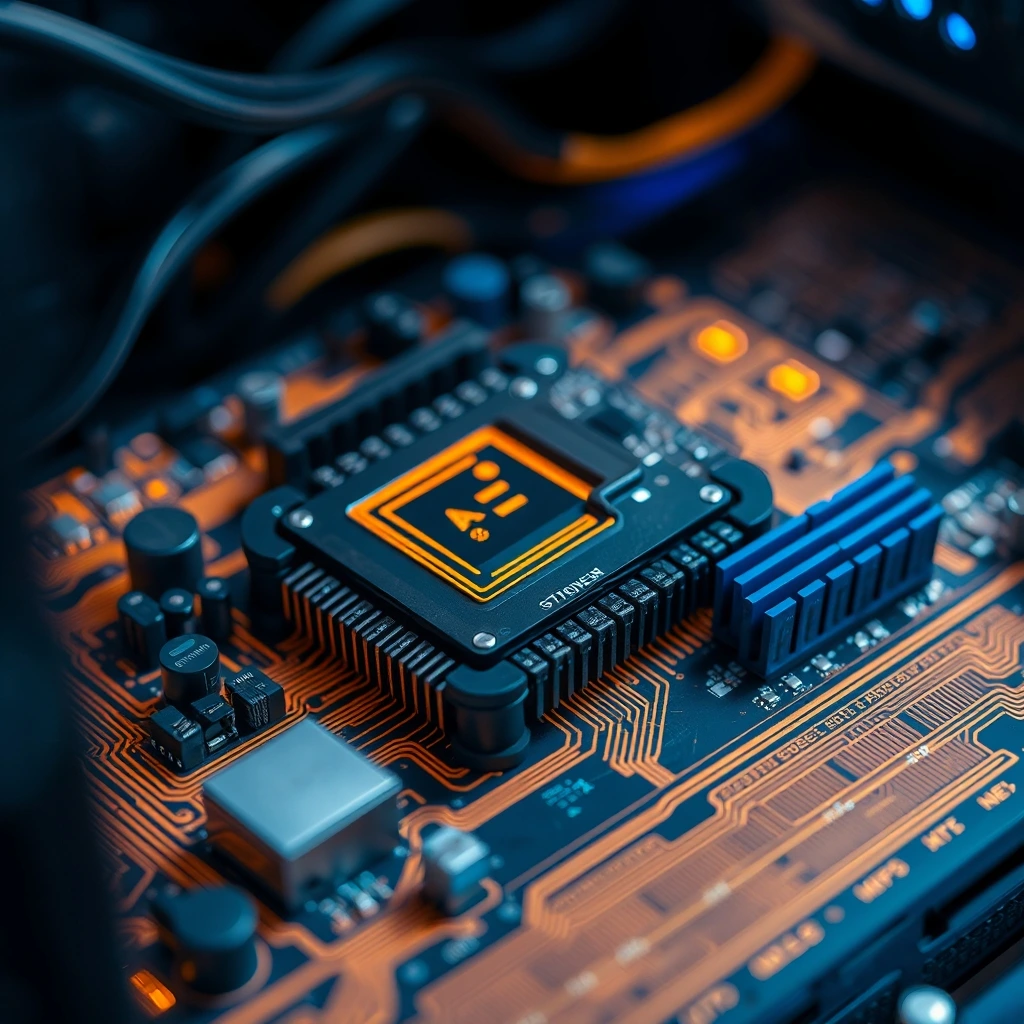
- Thermal Realism: Pure compute density has hit a hard thermal wall, forcing extreme reliance on optical interconnects and microfluidic cooling.
- Architecture Shift: Massive monolithic dies are dying out, replaced by intricate chiplet arrangements and non-volatile in-memory compute blocks.
- Economic Strain: Fabrication costs have skyrocketed to the point where only hyper-scalers can afford custom silicon tape-outs.
Look past the marketing hype sheets from major fab houses. The brutal truth of 2026 is that we are no longer constrained by algorithmic ingenuity, but by sheer electrical current and heat dissipation. Let's be candid: building a bigger neural network is easy. Keeping the silicon powering it from melting your server rack is where the real engineering nightmare begins.
The Thermal Crisis No One Wants to Discuss
We hit the power wall hard. Standard air cooling cannot keep up with clusters pushing kilowatts per socket. Engineers now face staggering thermal densities that defy traditional cooling paradigms. When your primary bottleneck is moving heat away from a square centimeter of silicon faster than it generates, traditional motherboard layouts break down completely.
To survive this era, hardware designers are radically rethinking how power enters the chip. Vertical power delivery has emerged as the default standard, routing current from the backside of the wafer rather than choking the top-side routing layers. Without this separation, current simply cannot reach the core transistors without massive voltage drop.
Chiplets, Interposers, and the Death of Monolithic Dies
Building massive single-die processors is economically and physically unfeasible at the current nodes. Yield rates plummet when a die grows past a certain surface area. The industry has universally embraced modularity.
- High-Bandwidth Interconnects: Silicon bridges connect compute tiles with minimal latency penalties.
- Heterogeneous Integration: Placing SRAM, logic, and analog I/O on separate optimized nodes rather than one compromised wafer.
- Advanced Packaging: Utilizing hybrid bonding to achieve sub-micron pitch connections between stacked dies.
| Aspect | Traditional Approach | Modern Solution |
|---|---|---|
| Die Architecture | Monolithic massive single die | Modular multi-die chiplets |
| Cooling Strategy | High-velocity air cooling | Direct-to-chip liquid and microfluidics |
| Memory Integration | Off-die HBM stacks | Monolithic 3D-stacked in-package memory |
In-Memory Compute: Leaving Von Neumann Behind
Moving data back and forth between memory and compute units burns staggering amounts of power. The latency penalty of the memory wall has forced a permanent architectural pivot toward processing data directly inside the memory array.
Resistive RAM and magnetic tunnel junction cells are finding real production deployments in edge and data center accelerators. By performing matrix multiplications directly via analog physics inside the memory cells, the processor eliminates the energy-hungry data shuttle entirely.
Do not evaluate enterprise AI silicon solely on theoretical peak FLOPS. Ask vendors for sustained performance metrics under thermal throttling conditions running real-world sparse attention models. Peak numbers mean nothing if the chip clocks down by half after ninety seconds of continuous inference.
The Photonics Revolution Arrives
Copper wiring is officially obsolete for inter-rack communication. Photonic interconnects have moved out of academic labs and directly onto the silicon interposer. Modulating data onto laser light pulses cuts latency to absolute minimums while virtually eliminating resistive signal loss over distance.
Integrating optical transceivers directly beside the processing cores requires unprecedented manufacturing precision. Packaging engineers now work hand-in-hand with photonics experts to align microscopic laser diodes with passive waveguide structures on the same silicon substrate.
Frequently Asked Questions
Why are custom ASICs replacing general-purpose GPUs in many enterprise pipelines?
Custom application-specific integrated circuits strip away all the general-purpose overhead, such as legacy graphics pipelines and universal instruction sets, leaving pure, hyper-optimized matrix multiplication hardware. This delivers superior energy efficiency for specific transformer workloads.
Is neuromorphic computing finally ready for mainstream deployment?
Event-driven neuromorphic architectures are finding massive utility in edge sensors and robotics where low-latency, sparse data streams demand milliwatt-level power envelopes. However, for massive large-language model training, traditional tensor architectures still dominate due to software ecosystem maturity.